News
Ultra High Speed Unpatterned Wafer Defect Inspection Tool
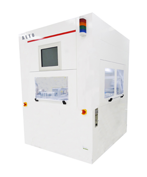
Santa Clara, Calif., Dec. 4, 2012-- Alto Inspection today announced its next-generation in-line unpatterned wafer inspection tool, the ALTO SD-6000. Developed specifically for transparent wafers surface inspection, the ALTO SD-6000 also provides the highest throughput available in the market to meet the growing integrated inspection demand.

The tool has a unique and sophisticated image analysis and defect classification, its defect library allows the users to classify the defect and customize the parameters with very little effort. The system offers from 10 to 1 micron resolution to accommodate each customer's inspection and throughput needs. It is flexibly designed with bridge capability from 2”-4”, 4-6”, 6"-8”. It also offers 2-side inspection capability
with its wafer flipping feature. The recipe-driven and user-manipulated binning and sorting capability significantly improves the operation efficiency and productivity.
The ALTO-SD-6000 is the best choice for sapphire, quartz, compound, micro-electro-mechanical systems (MEMS). The tool supports thin, warped wafers also thick wafers (from 50 microns to 1.5 mm). The tool's throughput allows 100% wafer inspectionis for a Total Quality Control. It’ a the tool to improve the manufacturing yield yet with very affordable Cost of Ownership.
EVENTS
Visit us at below shows
July 9-11, 2013, San Francisco, Semicon West, south hall, # 2041
Questions?
write to us if you have any questions or you would like to request technical details or arrange a demo.
Inquiry