In-Line Wafer Surface Defect Inspection
ALTO-SD-150/200 For Transperent Wafers
ALTO-SD series is an In-line inspection system supplying high throughput, full surface defect inspection for all kinds of wafers including silicon, quartz, sapphire, compound and MEMS wafers. High-resolution camera optics plus LED illumination guarantee reliable detection of all local defects. It inspects defect size of 1~ 10 microns, configurable inspection resolution to optimize defect size vs. throughput. The system combines high-precision measurement, powerful data analysis and user-friendly operations.
Prcoess Time by resolution (optional 1 micron resolution)
Sec/per wafer |
10 micron | 5 micron | 2.5 micron |
|---|---|---|---|
| 2" wafer | 2 sec | 5 sec | 10 sec |
| 4" wafer | 4 sec | 10 sec | 20 sec |
| 6" wafer | 5 sec | 15 sec | 30 sec |
Systematic Defect Tracking
accurate defect capturing and classifcation
Sophisticated image analysis and defect classification, e.g. detection of Cracks, edge chips, scratches, stones, shells, holes, stains, bright and dark spots, dirt, particles, dabs, fatty residues . optional non-contact, 2-sided wafer ID reading/inspection capability.
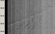
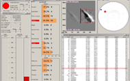
Position and type of the defects are indicated as symbols in the defect map. The exact defect data (position, size, type and further properties) are given in the defect list. All defects can be visualized by bit maps asillustrated on the top picture on left hand side.
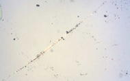
This ALTO-SD system is an affordable solution to imporve your quality control by avoiding the the mis-detection by microscope-reading and enabling 100% product examination. Illustrated on bottom left picture is microscope image of the sme area of interest (2.5X magnification).
Intelligence
user recipe driven
parameter set allows easy adaptation to customer specific requirement:
- Customizable layout and parameter
- All relevant info in a single view
- OK-NG indicator via “traffic light
- Global Event and Defect counter
- Simple Defect type represented by by colored symbols
- “Mouse Click” on defect on the map to get detailed information
Questions?
write to us if you have any questions or you would like to request technical details or arrange a demo.
Inquiry