Wafer Thickness, TTV, Bow and Warpage
handles 25 micron wafers
ALTO-TTV family offers the speedy measurement of wafer geometry parameter, more importantly, we can automate the tool to handle from thin wafers to perforated, warped, bumped, and tape-framed wafers. optional sorter and shipping jar unpacking function available.
measurement specification
specification |
wafr thickness | wafer ttv |
|---|---|---|
| speed of measurement | 3 sec | <20 sec |
| range of measurement | 25-1000 microns | accuracy | 0.25 microns | 0.05 micron |
| repeatability | 0.10 microns | 0.02 micron |
Multi-functional
non-contact, high reliability measurement
ALTo-TTV automatic measuring system is economic, small foot-print with multiple hardware and metrology optins to meet each customers requirement
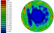
Illustraed picture (LEFT) is a TTV map of 200mm Silicon Wafer. TTV is acquired by measuring the capacitance with a propreitary Resonance Method. Single Sensor 1000 points used the , TTV = 6.70 micron
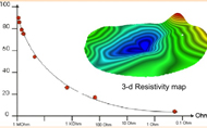
Aside from wafer thick ness and ttv, the tool has options to measure the edge of a wafer, check the conductivities (N/P) and the substrate resistance as the 3D map shows (Left)
Profiling
delicate wafers
When wafers get fragile and automation is a must for production need. alto-ttv is the choice that can help you deal with the delicate wafers.
- from Si, sapphire, to compound wafers
- wafer thickness, Total thickness variations (TTV)
- warp, bow, sag
- wafer edge profiling
- resistance
- conductivity (P/N)
Questions?
write to us if you have any questions or you would like to request technical details or arrange a demo..
Inquiry